First Steps
The development process for a flink system has two main parts: the configuration of the FPGA with the desired functions and the writing of the application software on the processor side.
FPGA Side
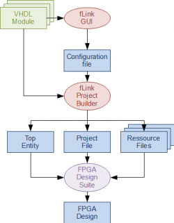
Ready-made modules realising functions such as PWM or analog inputs are available and can be stitched together. Available functions can be found in Available Subdevices. A suitable interface to the processor must be choosen as well. The figure below shows the workflow.
The VHDL modules can be found in flink VHDL. The blue boxes denote automatically created files. The red boxes symbolise planned components which are not yet available. For the time being you have to manually configure your VHDL project.
Currently we support Altera and Xilinx FPGAs with its associated IDE (Quartus II, Vivado 2016.1 or newer).
Processor Side
The processor will be connected to the FPGA through a certain interface. On a Linux system suitable kernel modules enable this communication (see flink Linux Kernel Modules). You can write your application in user space using the API offered by the flink Userspace Library. The figure below shows the workflow.
Here again, blue boxes denote automatically created files.

