User Tools
Sidebar
flink_example_1
This is an old revision of the document!
flink on Phytec PCM032 Board (mpc5200)
The following example describes in detail how a Phytec PCM032 Board containing a mpc5200 and a FPGA is configured to be used with flink. The FPGA will contain a single channel PWM module and a single channel GPIO modul. flink was tested with the FPGA on the mpc5200io module as well as with an external FPGA connected through a SPI interface.
External FPGA connected through SPI interface
The pmc5200 offers a dedicated SPI (8 bit transfers) which can be routed onto the pins of the timer group or the PSC3 group. The PSC1, PSC2, PSC3 or PSC6 can operate as an SPI with 32 bit transfers.
Setup
- Configure the board with a working Linux kernel and root file system or use the system described in Installation von Emdebian Grip auf den Phytec phyCORE-MPC5200B. Make sure to have the SPI properly configured (enabled).
- Make sure that the device tree blob is up-to-date. It must contain a node for the hardware SPI (spi@f00) or a PSC-SPI (e.g. spi: psc@2000).
- Get necessary sources for the flink project.
git clone https://github.com/flink-project/flinkvhdl.git
git clone https://github.com/flink-project/flinklinux.git
git clone https://github.com/flink-project/flinklib.git
Configure the FPGA
Proceed as described in flink VHDL.
- In 5: add a block gpio and a block pwm to the system. Leave the standard values as they are except for the PWM module, whose base clock depends on your FPGA clock. Set
unique_idof the gpio subdevice to 0x20 and theunique_idof the pwm subdevice to 0x30. Also add a spi_to_avalon module. Use SPI settings as given in the picture below.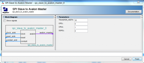 Adding an interface block
- In 6: set the
unique idof the info subdevice to 0x10. Convert a chosen string into a digital value and enter this value in the fielddescription.dev_sizeshould be 0x1c0 for our configuration. - After 10: the system should now look like:Invalid LinkComplete system
TODO improve picture

Connect the FPGA with the SPI pins on the mpc5200.
Loading the kernel modules
There are several ways to properly drive the SPI from the mpc5200.
Configure pin multiplexing
The hardware SPI and can be routed onto several different pin groups. The PSC-SPI needs configuring of the port configuration register. Our current UBoot does not yet fully suppport device tree configuration, it must be done manually. These actions could be done in a board initialization file. We prefer to put it directly into the mod_init function of the flink_spi driver. The code below sets to port configuration register so that one of the PSC's pin groups runs in SPI mode.
	// use these declarations for platform specific initialization
	static const struct of_device_id mpc52xx_gpio_simple[] = {
		{ .compatible = "fsl,mpc5200-gpio", },
		{}
	};
	struct mpc52xx_gpio __iomem *gpio;
	struct device_node *np;
	u32 portConfig;
	u8 pscNum = 2;	// set to 1,2,3 or 6

	// use in case a PSC serves as SPI
	// set port configuration register of mpc5200
	np = of_find_matching_node(NULL, mpc52xx_gpio_simple);
	gpio = of_iomap(np, 0);
	of_node_put(np);
	if (!gpio) {
		printk(KERN_ERR "%s() failed, expect abnormal behavior\n", __func__);
		return -1;
	}
	portConfig = in_be32(&gpio->port_config);
	#if defined(DBG)
		printk(KERN_DEBUG "[%s] Current port config = 0x%x\n", MODULE_NAME, portConfig);
	#endif
	if (pscNum == 6) {
		portConfig |=  0x00700060;	// PSC6 is Codec/SPI
	} else if (pscNum >= 1 && pscNum <= 3) {
		portConfig &= ~(7 << ((pscNum-1)*4));
		portConfig |=  6 << ((pscNum-1)*4);
	} else {
		printk(KERN_ERR "[%s] Wrong PSC number\n", MODULE_NAME);
		return -1;
	}
	out_be32(&gpio->port_config, portConfig);
	#if defined(DBG)
		printk(KERN_DEBUG "[%s] New port config = 0x%x\n", MODULE_NAME, portConfig);
	#endif
	iounmap(gpio);
Similarly you could configure the PSC3 group that the hardware SPI is output on the pins PSC3_6 .. PSC3_9. In our system this is already done by UBoot.
Build into kernel
Compile kernel modules (see flink Linux Kernel Modules) and add them to your kernel image. Add a subnode flink_spi to your device tree under the node spi. In the compatible statement you must specify which protokoll driver to load (compatible = “flink_spi”). You can also specify the clock frequency. When booting the SPI-subsystem will automatically load a master driver (spi-mpc5200 or spi-mpc5200-psc) and the protokoll driver flink_spi.
Load manually
When loading the driver manually add the following code to the mod_init function of the flink_spi driver.
	struct spi_master *master;
	struct spi_device *dev;
	master = spi_busnum_to_master(num);	// use bus number of master
	if (!master) {
		printk(KERN_ERR "[%s] No master for this bus number\n", MODULE_NAME);
		goto exit;
	}
	dev = spi_new_device(master, &flinkInfo);
num must correspond to your master bus number. This will be 32766 for the hardware SPI and 1,2,3 or 6 for the PSC-SPI. You have to specify driver data as follows.
static struct spi_board_info flinkInfo = {
		.modalias = "flink_spi",
		.max_speed_hz = 2000000,
		.mode = SPI_MODE_1
};
When working with a PSC-SPI you would configure it to run with truly 32 bit transfers. Add the following lines:
	dev = spi_new_device(master, &flinkInfo);
	dev->bits_per_word = 32;
	spi_setup(dev);
Finally, compile kernel modules (see flink Linux Kernel Modules), transfer them to the target and load them:
insmod flink.ko
insmod flink_spi.ko
As we specified an info subdevice we can ommit the memory length when loading flink_lpb.ko.
flink library and application
Compile the flink library (see flink Userspace Library) together with several test applications. Transfer the library and the test application to the target. Make sure that your library path includes the actual location of your library. Run test applications such as lsflink, flinkdio or flinkpwm.
Onboard FPGA connected through Local Plus Bus
Setup
- Configure the board with a working Linux kernel and root file system or use the system described in Installation von Emdebian Grip auf den Phytec phyCORE-MPC5200B
- Make sure that the device tree blob is up-to-date. It must contain a node for the FPGA sitting on the local plus bus.
- Get necessary sources for the flink project.
git clone https://github.com/flink-project/flinkvhdl.git
git clone https://github.com/flink-project/flinklinux.git
git clone https://github.com/flink-project/flinklib.git
Configure the FPGA
Proceed as described in VHDL.
- In 5: add a block gpio and a block pwm to the system. Also add a lpb_mpc5200b_to_avalon module. Leave the standard values as they are except for the PWM module, whose base clock should be 33000000. Set
unique_idof the gpio subdevice to 0x20 and theunique_idof the pwm subdevice to 0x30Invalid LinkAdding an interface blockTODO improve picture
- In 6: set the
unique idof the info subdevice to 0x10 and the …. - After 10: the System should now look like:Invalid LinkComplete system
TODO improve picture
- In 15: assign the pins as follows:
| signal | dir | pin |
|---|---|---|
| clk_clk | in | PIN_H2 |
| lpb_ack_n | out | PIN_T11 |
| lpb_ad[31] | bidir | PIN_T6 |
| lpb_ad[30] | bidir | PIN_N8 |
| lpb_ad[29] | bidir | PIN_R9 |
| lpb_ad[28] | bidir | PIN_T9 |
| lpb_ad[27] | bidir | PIN_R8 |
| lpb_ad[26] | bidir | PIN_T8 |
| lpb_ad[25] | bidir | PIN_L8 |
| lpb_ad[24] | bidir | PIN_L7 |
| lpb_ad[23] | bidir | PIN_R7 |
| lpb_ad[22] | bidir | PIN_T7 |
| lpb_ad[21] | bidir | PIN_R5 |
| lpb_ad[20] | bidir | PIN_T5 |
| lpb_ad[19] | bidir | PIN_R4 |
| lpb_ad[18] | bidir | PIN_T4 |
| lpb_ad[17] | bidir | PIN_P4 |
| lpb_ad[16] | bidir | PIN_P5 |
| lpb_ad[15] | bidir | PIN_R3 |
| lpb_ad[14] | bidir | PIN_T3 |
| lpb_ad[13] | bidir | PIN_P11 |
| lpb_ad[12] | bidir | PIN_N11 |
| lpb_ad[11] | bidir | PIN_L11 |
| lpb_ad[10] | bidir | PIN_M11 |
| lpb_ad[9] | bidir | PIN_R14 |
| lpb_ad[8] | bidir | PIN_T14 |
| lpb_ad[7] | bidir | PIN_R13 |
| lpb_ad[6] | bidir | PIN_T13 |
| lpb_ad[5] | bidir | PIN_R12 |
| lpb_ad[4] | bidir | PIN_T12 |
| lpb_ad[3] | bidir | PIN_P13 |
| lpb_ad[2] | bidir | PIN_P12 |
| lpb_ad[1] | bidir | PIN_K10 |
| lpb_ad[0] | bidir | PIN_K11 |
| lpb_ale_n | in | PIN_R11 |
| lpb_cs_n[0] | in | PIN_N10 |
| lpb_int | out | PIN_R6 |
| lpb_oe_n | in | PIN_L9 |
| lpb_rdwr_n | in | PIN_L10 |
| lpb_ts_n | in | PIN_T10 |
| reset_reset_n | in | PIN_N9 |
The pins for the PWM output and the GPIO have to be assigned according to your hardware. The FPGA can be loaded through the onboard PROM or through serial loading from the processor, see Installation von Emdebian Grip auf den Phytec phyCORE-MPC5200B.
Loading the kernel modules
Compile the Linux kernel modules (flink Linux Kernel Modules), transfer them to the target and load them with
insmod flink.ko
insmod flink_lpb.ko
As we specified an info subdevice we can ommit the memory length when loading flink_lpb.ko.
flink library and application
This step is the same as described under using the SPI.
flink_example_1.1427526000.txt.gz · Last modified: (external edit)
Page Tools
Except where otherwise noted, content on this wiki is licensed under the following license: CC Attribution-Share Alike 4.0 International
